01
Rare-earth composition & ratios
Change host and dopant combinations to shift excitation pathways, emission wavelengths, intensity ratios and interaction between energy levels.
Intelligent Material Solutions develops intellectual property related to energy-converting materials. NovaVera Corporation is the commercialization arm for the technology.
Intelligent Material connects the physical world with the digital world. Our inert rare-earth crystals convert energy into measurable information. We engineer the crystal itself, changing how it interacts with light, energy, magnetic fields and its surrounding environment.
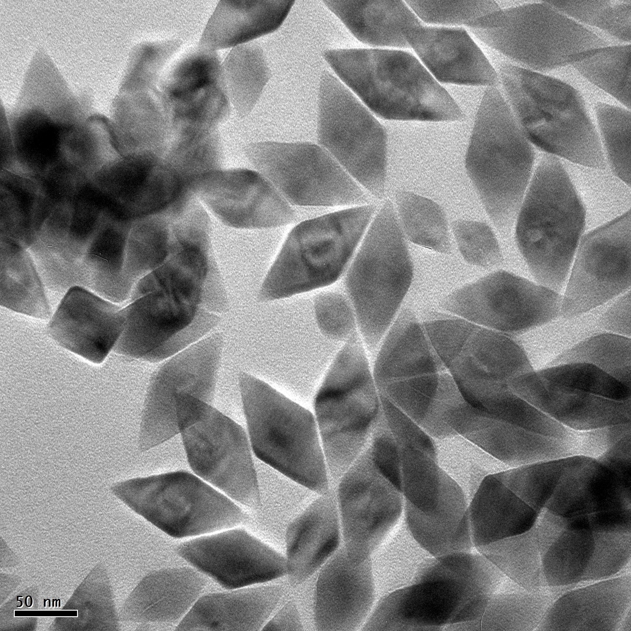
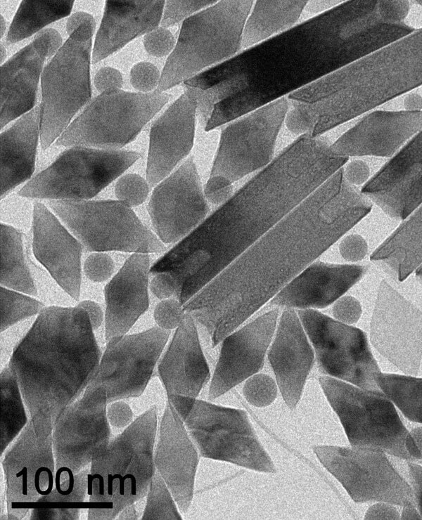
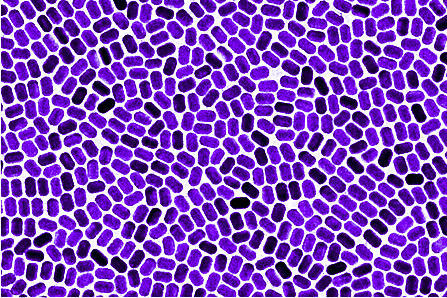
Private demo · partners only
Spin a crystal code, try a fake, then build core/shell crystals layer by layer and watch the combinations go through the roof. These interactive demos are open to partners.
v@nova-vera.com
Reading Intelligent Material does not need a lab instrument. It needs the same kind of tiny sensor phones use to measure distance, with two changes: a filter made for our crystals and a gate timed to their glow. The emitter can be swapped too, to any wavelength our crystals answer, or several emitters can share one chip.
Some versions split the detector into 4 × 4 or 8 × 8 zones. Each zone counts photons on its own, so one chip can see several stripes, or a whole two-dimensional code, in a single look.
A stock chip listens for nanoseconds to measure distance. Ours waits until the laser echo is long gone, then listens from microseconds to milliseconds: the sweet spot where our crystals are still glowing and nothing else is.
Built from the same class of part as commercial multizone time-of-flight sensors, such as STMicroelectronics' VL53 family (940 nm VCSEL, single-photon avalanche diode array, up to 8 × 8 zones). The bespoke filter, alternative or multiple emitters and microsecond-to-millisecond gating are IMS modifications; the ≈ $1 figure is an IMS cost target, not a vendor price.
The most powerful use of Intelligent Material is becoming part of the product itself. Once the crystal is inside a polymer, coating, ink, oil, fiber, biological assay or other compatible system, the product carries a persistent engineered response from the moment it is made.
We can encode information into composition, structure, wavelength response, lifetime, excitation dependence, magnetic behavior and core/shell interactions.
The result is a material that can convert energy, carry information and remain physically connected to the thing being measured, authenticated or controlled.
IMS treats each crystal as a multidimensional information carrier whose response can be engineered for a specific purpose.
Change host and dopant combinations to shift excitation pathways, emission wavelengths, intensity ratios and interaction between energy levels.
Control particle dimensions, crystal facets and uniformity to influence optical behavior, surface interactions, processing and self-assembly.
Engineer rise, decay, persistence and lifetime behavior so time itself becomes another dimension of the material identity.
Combine optical and magnetic behavior to create materials that can be identified optically while responding to magnetic fields or separation methods.
Separate, couple or enhance functions across nanoscale interfaces, including energy transfer, isolation, surface chemistry and plasmonic effects.
Vary excitation power density and measure how emission responds. The intensity-dependent response curve becomes another way to identify the material.
Rare-earth ions occupy discrete electronic energy states. By choosing the host, dopants and concentrations, we engineer which wavelengths are absorbed and which wavelengths are emitted.
Two or more lower-energy excitation events can populate higher excited states. The material can then emit a shorter-wavelength photon, allowing invisible near-infrared excitation to produce visible light.
A higher-energy photon is absorbed and the excited ion relaxes before emitting at a longer wavelength. We can engineer this response across UV, visible and infrared regions.
Crystal Designer is a separate IMS tool for exploring the material variables that control optical behavior. Instead of presenting a fake software interface here, this page shows the design logic and then takes you directly into the real tool.
Define the physical and chemical environment around the active ions.
Select activators and sensitizers and tune their concentrations.
UV, visible, 808, 940, 980, 1550 nm and other optical inputs.
Spectrum, lifetime, power-density response, magnetics and core/shell behavior.
Christopher B. Murray is an inventor on the IMS / University of Pennsylvania uniform-crystal patent family. He was also first author, with David Norris and Moungi Bawendi, on the landmark 1993 paper describing a controlled synthesis of nearly monodisperse semiconductor nanocrystals.
The 2023 Nobel Prize in Chemistry recognized Moungi Bawendi, Louis Brus and Aleksey Yekimov for the discovery and synthesis of quantum dots. The Nobel background specifically identifies Bawendi's 1993 advance in producing high-quality quantum dots with controlled size. IMS's work applies the same broader lesson to a different materials platform: precise control of nanoscale composition, size and architecture creates precise control of material behavior.
Synthesis and characterization of nearly monodisperse CdE semiconductor nanocrystallites.
Read the paper · 2023 Nobel Prize context
IMS / Penn patentMorphologically and size uniform monodisperse particles and their shape-directed self-assembly. Inventors include Howard Bell, Joshua Collins, Xingchen Ye and Christopher Bruce Murray.
Private demo · partners only
Two peer-reviewed papers co-authored by IMS, in PNAS and Nature Chemistry, with electron micrographs, simulation movies and an interactive look at how crystal shape is controlled. Open to partners.
v@nova-vera.com
The portfolio spans uniform particles and assemblies, temporal authentication, rare-earth materials in articles and systems for identifying Intelligent Material from its engineered emission response.
Monodisperse particles and shape-directed self-assembly developed with the University of Pennsylvania.
Related claims involving up- and down-converting particles, polyhedral morphology and organized superlattices.
Authentication using engineered temporal characteristics of the emission response.
IR-blocking inks incorporating rare-earth Intelligent Material for article and transaction-card authentication.
Methods and systems for identifying Intelligent Material from changes in emission response under controlled illumination.
Start with the material itself. IMS can help define the excitation, emission, temporal, power-density, magnetic and structural response needed for the application.
Work with IMS ISO 9001:2015 CertifiedQuality management system · SGS certificate US23/00000276 · valid to June 2029